Deep Learning-Based Semiconductor Product Inspection
A lightweight twin network for real-time defect detection in semiconductor IC substrates.
Overview
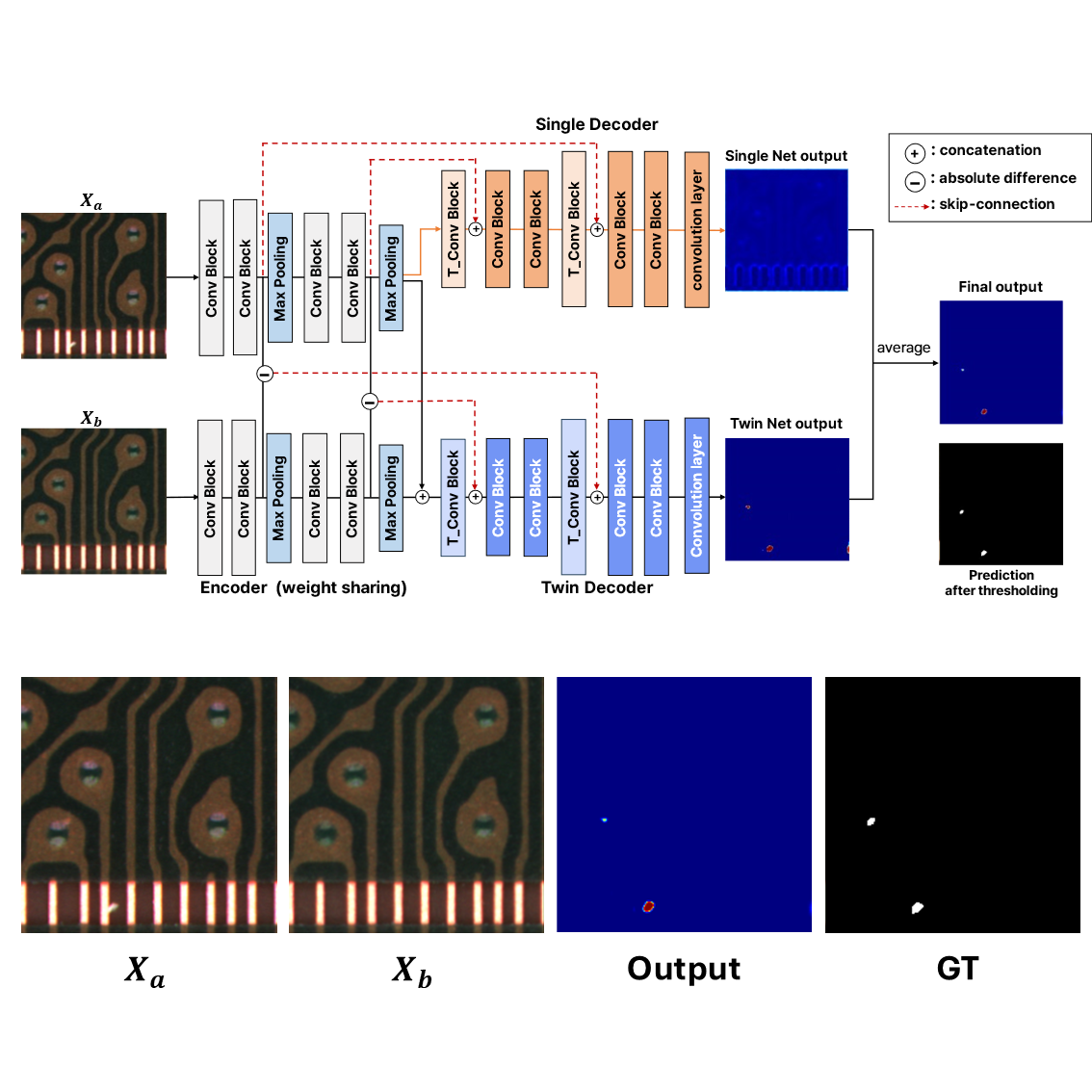
For my Master’s degree thesis (Yoon, 2024), I developed a lightweight twin network-based defect detection system for IC substrates. This system is designed to be robust against mis-registration and characteristic differences, ensuring high accuracy and reliability in real-time semiconductor inspections.
Objectives
-
To design a robust defect detection system for semiconductor inspection: This research focuses on inspecting IC substrates, leveraging their repetitive patterns to implement comparison-based inspection techniques that detect changes between test and reference images.
-
To minimize mis-registration errors while maintaining lightweight computational requirements: While twin network structures, which use two identical encoders for feature extraction and comparison, are commonly used for change detection, they are prone to pseudo changes and mis-registration errors. These issues complicate the detection of micro defects critical for accurate inspections.
-
To apply state-of-the-art deep learning techniques for real-time performance: Existing methods, such as co-attention modules and similar architectures, demand significant memory, computational resources, and processing time, making them unsuitable for deployment in real industrial environments.


Key Contributions
- Developed a Siamese Network-based architecture optimized for defect detection in repetitive patterns: Proposed C-TSNet, a hybrid architecture combining twin and single networks to enhance robustness against mis-registration and color variations, while maintaining low computational latency.
- Enhanced robustness using advanced attention mechanisms: Introduced CC-TSNet, which incorporates a channel co-attention module to further improve resilience to characteristic differences.
- Achieved real-time performance with lightweight computational requirements: Designed the architecture to be efficient for deployment in industrial settings, ensuring fast and accurate defect detection.


Technologies and Tools
- Frameworks: TensorFlow, PyTorch
- Key Techniques:
- Siamese Networks (also known as twin network)
- Change Detection
- Attention Mechanisms
- Hardware: NVIDIA GPUs for accelerated training and inference
Results
- Superior performance on real-world industrial datasets: Validated the proposed methods on an IC substrate dataset, outperforming traditional models like U-Net and Base-Twin networks in terms of F1-scores and false positives.
- Improved robustness against pseudo-changes: The integration of the channel co-attention module significantly enhanced the model’s ability to handle characteristic differences, reducing false positive rates.
- Real-time suitability: Achieved accuracy comparable to module-based methods, with only one-third of the computational latency, making the system highly effective for real-time manufacturing processes.


Additionally…
- Exploration of advanced techniques: Beyond the main contributions, I explored various advanced deep learning methods, including Knowledge Distillation and Vision Transformers (ViT). While these approaches showed promise, they revealed limitations when applied to the specific challenges of IC substrate inspection.
- Efforts to improve single network performance for non-repetitive patterns: Recognizing the need for a solution in cases where products lack repetitive patterns, I focused on enhancing single network performance using ViT. Although the experiments did not yield the desired results, they offered valuable insights into the difficulties of defect detection in non-repetitive contexts.
- Future potential: These explorations highlight opportunities for further research. Perhaps someday, I will revisit these techniques to develop more robust solutions for diverse inspection scenarios.
- I labelled more than 100,000 images for the project🤪